|
Key Features
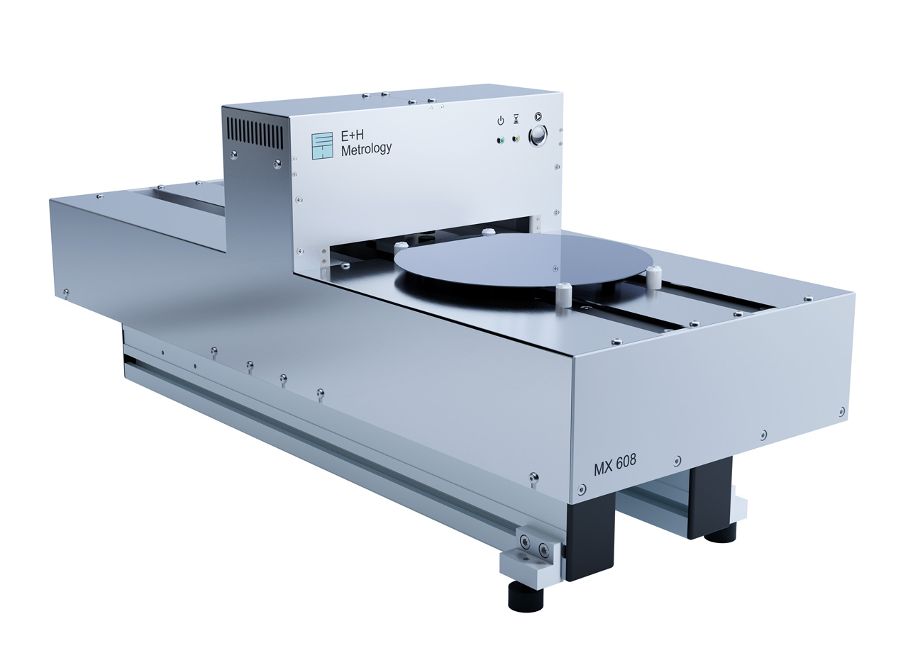
• All-in-One Measurement: Simultaneously measures thickness, resistivity, and TTV of 150mm and 200mm silicon wafers
• Non-Contact Technology: Utilizes advanced thickness sensors, resistivity sensors, and P/N dopant detection to protect wafer surfaces
• Fully Automated Scanning: Wafer is automatically loaded and scanned along its centerline, with lateral resolution up to 1 mm
• Multi-Angle Inspection: Automatic wafer rotation for up to 18 scans ensures complete coverage and accurate measurement results
• Software Integration: Works with MX-NT operating software for efficient data analysis and control
• System Connectivity: Connects to PC via serial interface and supports integration into automated robotic sorter systems
• Compact Desktop Design: Small footprint and easy operation for use in laboratories, R&D, and production lines
|