NEWS
2026.09.24
BlogsNow Available from Chunson | AST Advanced Optical Metrology, Inspection & Infrared Imaging Solutions
Chunson is pleased to introduce advanced inspection and metrology solutions from Advanced Spectral Technology, Inc. (AST), USA, further expanding our capabilities in precision metrology and defect inspection for semiconductor, MEMS, optoelectronics, and advanced packaging applications.
AST specializes in multispectral imaging, automated inspection, and precision metrology technologies
AST integrates high-accuracy motion control, advanced optical design, and imaging technologies across the Visible, NIR, SWIR, and MWIR spectra. Its configurable platforms support applications ranging from R&D and process development to automated high-volume manufacturing.
Advanced Inspection & Metrology Solutions
· AST-VCSEL|VCSEL Optical Aperture Metrology System
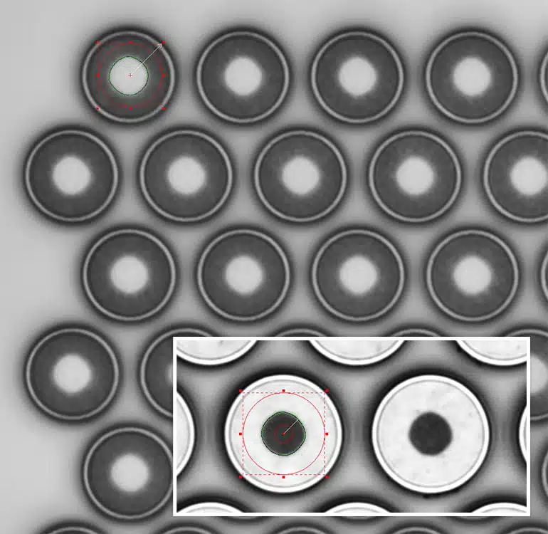
High-precision optical aperture metrology for VCSEL manufacturing, combining multispectral imaging and automation to measure aperture dimensions, geometry, position, and uniformity.
· AST-CDO|CD & Overlay Metrology System
Precision Critical Dimension and Overlay metrology for semiconductor processing, bonded wafers, advanced packaging, and layer alignment applications.
· AST-WDI|Wafer & Die Inspection System
High-precision wafer and die defect inspection for detecting microscopic particles, scratches, and pattern irregularities, supporting process control and yield improvement.
· AST-Zentura|Wafer Metrology System
Advanced wafer-level metrology designed to support precision measurement requirements in semiconductor manufacturing.
· AST-MEMS|MEMS Inspection Systems
Available in automated and workstation configurations, integrating Visible, NIR, and SWIR imaging technologies for subsurface visualization, dimensional metrology, and alignment verification of complex MEMS structures.
· AST-IR|NIR / SWIR Metrology & Inspection Systems
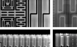
Advanced infrared imaging enables inspection through silicon and other wafer materials to reveal hidden structures, defects, and alignment issues for bonded wafers, bonded dies, MEMS, 3D stacking, wafer bonding, and failure analysis.
· AST-MWIR|Mid-Wave Infrared Imaging Systems
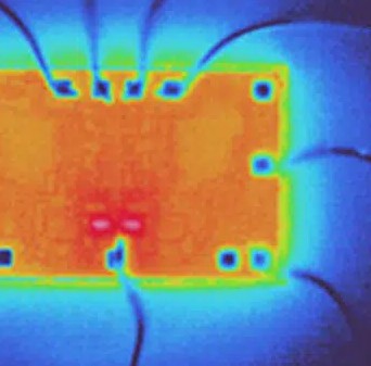
MWIR imaging and thermal analysis solutions available in workstation and benchtop platforms for semiconductor, material science, and other advanced applications.
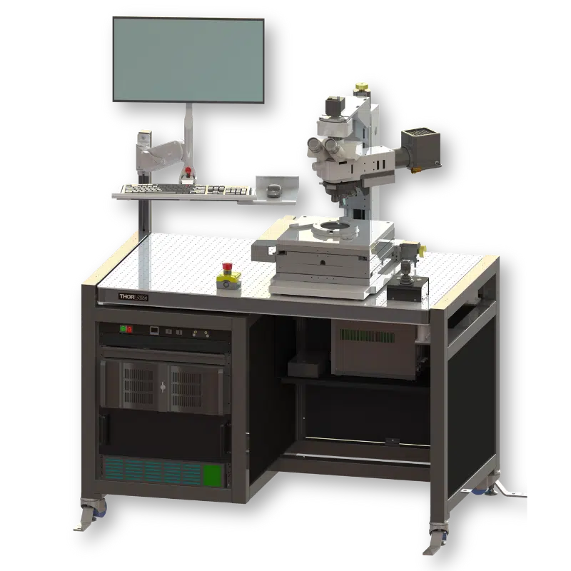
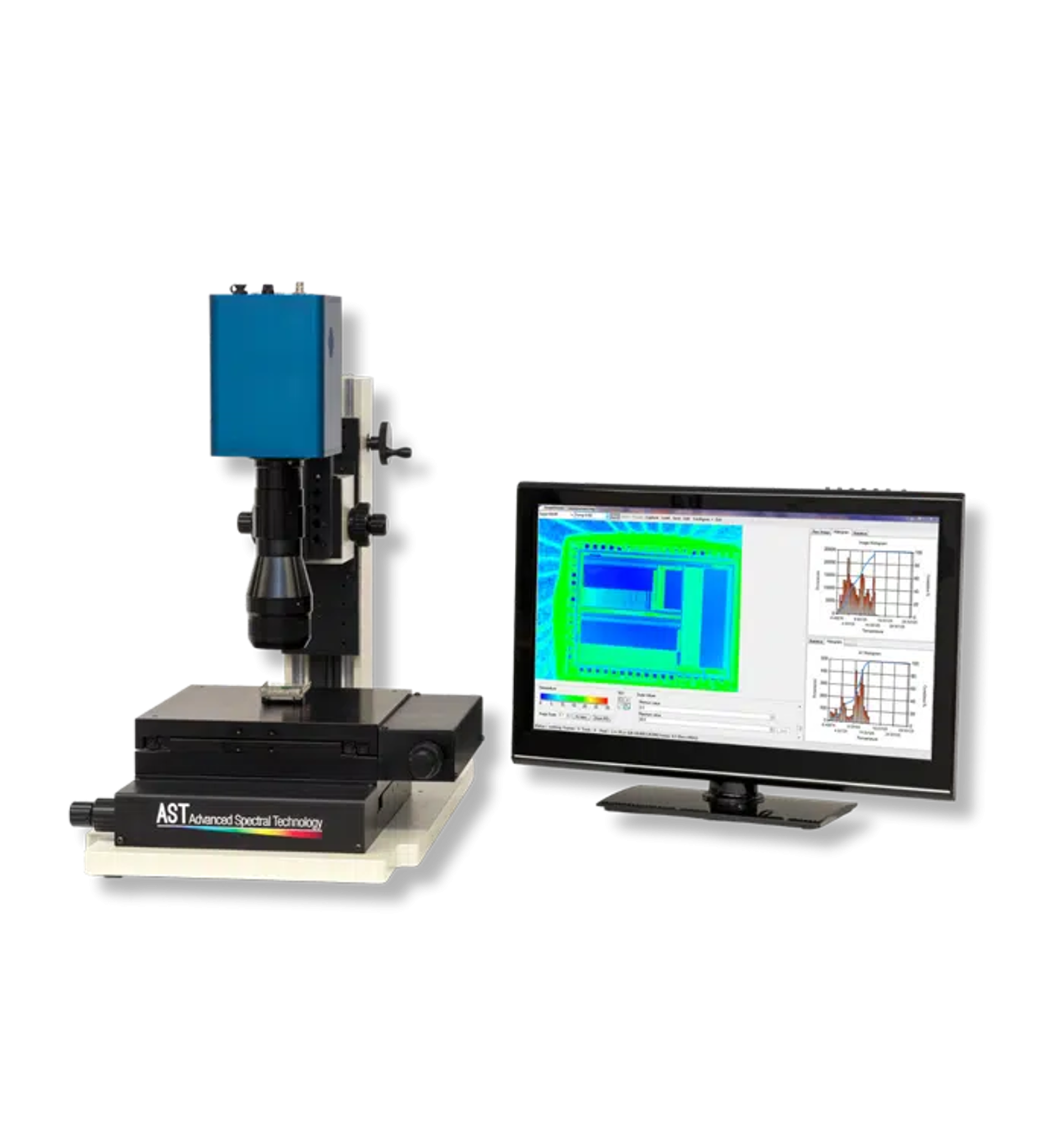

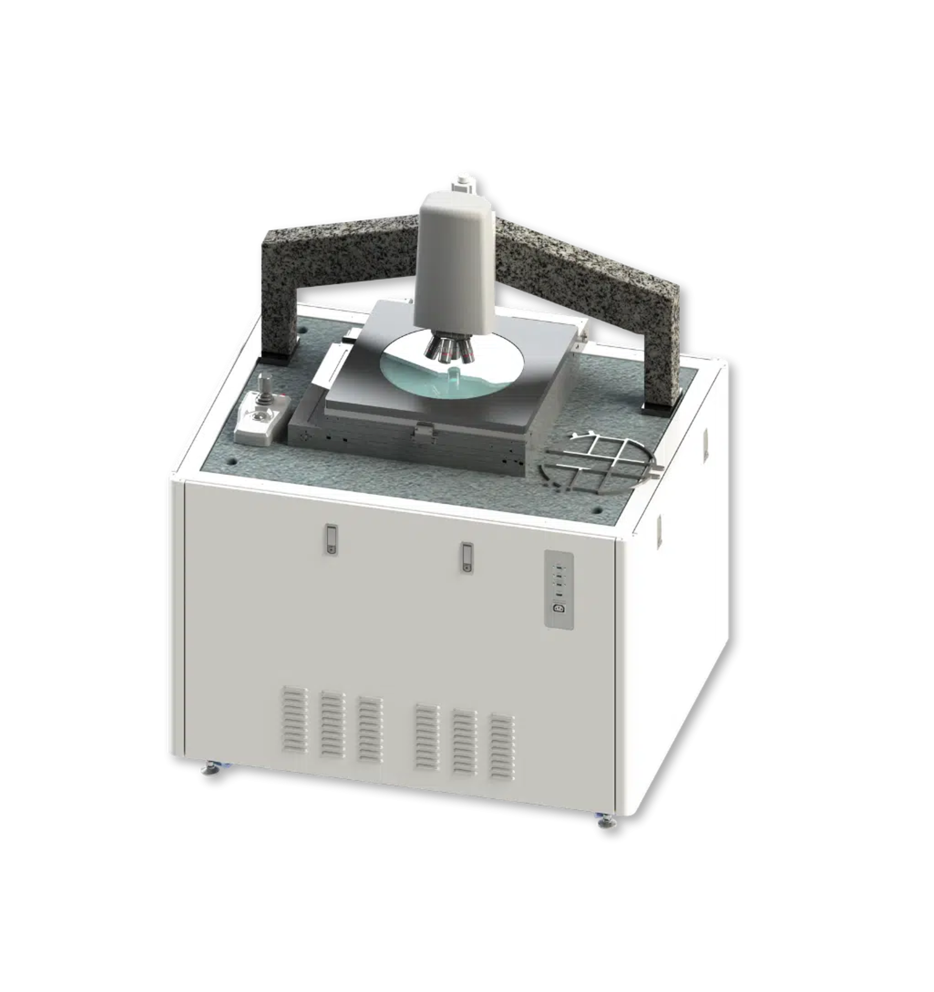
See Beyond the Surface
AST solutions support a broad range of markets, including Semiconductor / MEMS, Wafer / Die / Chip, VCSEL, Probe Card, and Data Storage manufacturing, with additional applications in medical and aerospace industries. By integrating precision optics, multispectral imaging, infrared technologies, and automation, AST provides flexible solutions for increasingly demanding inspection and process-control requirements.
Chunson continues to connect global advanced technologies with professional local technical support in Taiwan.
For applications involving Wafer / Die Inspection, CD & Overlay Metrology, VCSEL, MEMS, NIR / SWIR subsurface inspection, or MWIR thermal imaging.