
NEWS
- Home
- Exhibition information
- DIP-View VISION 300-M Debuts in Taiwan at SEMICON Taiwan 2025
2025.08.06
Exhibition informationDIP-View VISION 300-M Debuts in Taiwan at SEMICON Taiwan 2025
We warmly invite you to visit Chunson’s booth at SEMICON Taiwan 2025
France-based DIP-View will present its next-generation wafer metrology system – VISION 300 – M, making its first appearance in Taiwan. This advanced tool offers precise and reliable measurement solutions for cutting-edge semiconductor manufacturing processes.
|
|
|||
 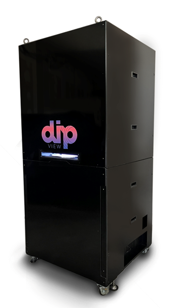 |
• Full-field one-shot measurement • SEMI compliant wafer metrology • Manual wafer loading for 200mm & 300mm • Accurate measurement of Bow, Warpage, TTV, LTV • Dual-side nano-topography analysis (Top & Bottom surfaces) |
||
| Get the entire wafer roughness within 20 seconds. | |||
|
About DIP-View DIP-View, based in France, is a technology company specializing in optical metrology for the semiconductor industry. With a focus on breakthrough innovations for nanometer-level measurements, DIP-View is actively expanding its presence across Asia. As a pioneer in high-resolution deflectometry for critical surface metrology applications, DIP-View also introduces the D-Surface View system, designed for wafers up to 300mm in diameter. It helps reduce manufacturing costs and improve yields in advanced semiconductor production. |
|||